Allegro PCB Designer
Constraint-driven PCB design
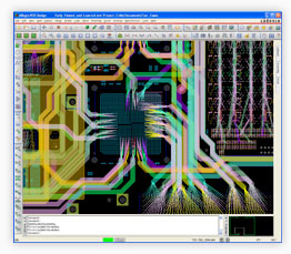
Allegro PCB Designer quickly takes simple or complex designs from concept to production in a constraint-driven design system. Its scalable based plus options model allows designers to cost-effectively match the technological and methodological needs of small to large companies and projects.
Speeds designs from placement and routing through to manufacturing with powerful features such as design partitioning, RF design capabilities, and interconnect design planning. Production-proven to increase productivity and help engineers quickly ramp up to volume production.
Oriented around team-based development, Allegro Design Authoring allows schematic designers and layout engineers to work in parallel. Users can capture physical and electrical constraints and assign design rules with the embedded Allegro Constraint Manager. Integrated with Allegro AMS Simulator for analog and digital simulation and SI analysis, Design Authoring also offers multiple options for FPGA integration.
Features/Benefits
- Provides a scalable, full-featured PCB design solution
- Enables a constraint-driven design flow to reduce design iterations
- Provides a single, consistent, front-to-back constraint management environment
- Delivers an integrated RF/analog design and mixed-signal design environment
- Provides interactive floorplanning and component placement
- Provides design partitioning for large, dispersed development teams
- Enables real-time, interactive push/shove etch editing
- Allows real-time plowing/healing with dynamic shape technology
- Manages net scheduling, timing, crosstalk, layer set routing, and geometric constraints
- Provides proven PCB Router technology for auto-routing of random signals
- Enables hierarchical Route Planning to accelerate design completion
- Shortens interconnect planning and routing time for dense designs with high-speed interfaces
- Outputs design data in a variety of manufacturing formats